


  |
|
Field-Programmable Gate Array (FPGA)
and Factory Programmed Application Specific Integrated Circuit
(ASIC)
Multiple FPGA architectures with different configuration technologies
Flexible general purpose data-path and control function where
user inserts memory elements as desired.
SRAM based (dynamic storage to personalize the logic function
of 4-5 input "look-up-table" blocks and their interconnection)
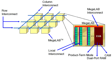
Xilinx, Altera, Lucent, and now Actel offer a variety of "course-grain"
architectures. The Xilinx XC4000 and new VIRTEX families utilize
an array of Configurable Logic Blocks (CLB) interconnected with
variety of pass-transistor switched lines and Programmable Switch
Matrices (PSM)
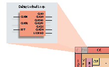
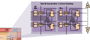
Xilinx VIRTEX architecture:
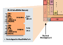 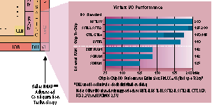
Altera APEX architecture:
Anti-Fuse based (one-time only personalization of unique fuse
elements to configure logic function blocks and their interconnect)
Actel offers a "fine-grain" architecture utilizing rows of
logic blocks which can be configured for a variety of logic
and memory functions 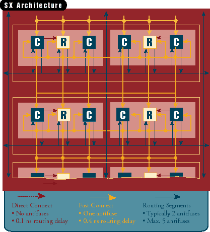
FLASH based (reconfigurable personalization of logic elements
and their interconnect)
Complex Programmable Logic Devices (CPLD) utilize a matrix of
"Sum-of-Products" logic function with a global interconnection
Very fast decode and FSM control functions for shallow logic
depth
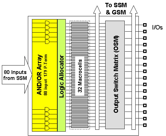
UV-PROM based (reconfigurable personalization of wide AND &
OR arrays with latched macrocell output)
FLASH based (reconfigurable personalization of wide AND & OR
arrays with latched macrocell output)
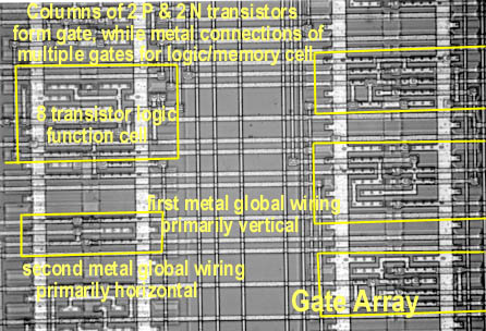
Mask Personalized Gate Array ASIC
Array of identical size P and N transistors personalized at
the contact and metal layers to form columns of various size logic
blocks spaced apart for vertical first metal and horizontal second
layer routing. Additional metal routing layers are used for global
signals and power/ground supply. New products utilize a "sea-of-gates"
architecture, where the area allocated for vertical metal routing
over unused transistors is flexible. Some large memory and logic
functions can be interconnected without wasting transistors under
routing tracks.
Simple double metal gate array:
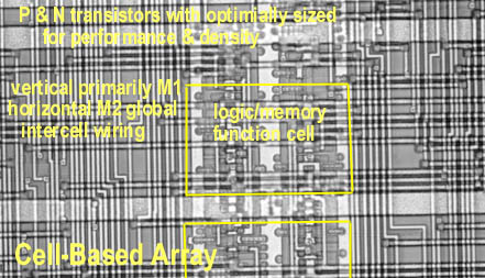
Mask Personalized Cell-Based ASIC
Columns of various logic and memory blocks with optimized P
and N transistor sizes personalized at all the mask layers. Optimum
performance and density are obtained compared to gate array architecture.
Multiple layers of metal routing are used to connect the transistors
within the block and route signals between blocks. With more complex
multi-level metalization deep-submicron IC processing, this approach
offers superior cost and performance as well as incorporating
hard IP macros.
Simple double metal cell-based array:
 |
Located in the heart of Silicon Valley,
California
 |